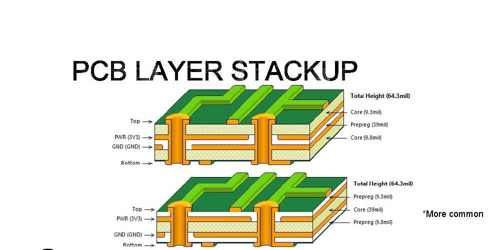
Printed Circuit Boards are designed to provide support to electronic components. Their designs vary depending on the devices, as some are more complex than others. The PCB is arranged in layers known as the PCB stack up. A good stack-up helps minimize radiation, the effect of external noise and enhance the electromagnetic compatibility of the entire board. The stack-up may have varying layers; for example, some are double layered while others are multiple. We look at PCB stack-up materials below.
Common PCB stack up materials
PCBs, come in different forms. They can be rigid or flexible, meaning the materials used are different. However, the fundamentals of a PCB stack-up are similar across all types. Below are the materials used in a typical stack-up.
1. Solder mask
Solder mask material is a polymer layer found on the outermost layer of the printed circuit board. It acts as a coating and protects the components, such as traces located on the first and last layers of the PCB. It is thin and appears green hence the green color found on PCB boards.
2. Copper foil
Copper is the main element in the PCB stack-up. Though other components may conduct electricity, copper is the primary conductor layer that facilitates the flow of current across the board. The major role of the copper layer within the stack is to form two planes; power and ground. On the PCB, copper creates the traces, and its thin nature allows for more routing. Thick copper foils enable more current to flow within it, making the electronic device more powerful.
3. FR4
This material doesn’t conduct electricity; hence current cannot flow through it. It is a substrate made of glass, and an epoxy laminate sheet and three different forms are available. They are halogen, high glass transition temperature, and standard. The combination of the two materials enhances its tensile strength, therefore suitable for providing mechanical support to the elements. FR4 is water-resistant, meaning it cannot be damaged if exposed to water
4. Prepreg
Prepreg material is a rare kind but exists in most stack-ups. It is impregnated with semi-liquid resin that flows when exposed to heat. The heated resin sticks together, making the Prepreg suitable for connecting the various stack-up layers during lamination. Like FR4, Prepreg offers good tensile and mechanical strength. It also comes in three forms; high, medium, and standard, depending on the thickness and layer arrangement.
5. Coverlay
Like Prepreg, coverlay adhesive is used to bind PCB layers. It holds them firmly on the board and keeps all components in their correct positions. The coverlay material is mainly polyamide used to develop flexible or flex-rigid PCBs. It has a similar role to the solder mask material, as it protects the components from any harm. Its chemical-resistant thus cannot be affected by corrosive elements.
Final word
The stack-up arrangement consists of the materials above. Each material has a definite role that enables the layer arrangement to remain firm and stay in place. The materials you choose when designing will determine the kind of stack-up you create and whether it’s fit to perform the desired task.
